Building the Gemini Stimdeck
Before we begin, please note, my intention with this blog post is, more or less, for it to be a project log and to show what went into making this project a reality. I understand that a lot of it is handwavy and sparse, but the scope of the project is just too big for me to cover everything in detail in a single blog post. So, I kind of just threw in everything and the kitchen sink.
What Inspired Me to Start
It's been a lifelong dream of mine, since I was a kid, to design my own electronics. I used to take apart every piece of electronics I could get my hands on. I'd look at the internals in awe and I knew I wanted to know more.
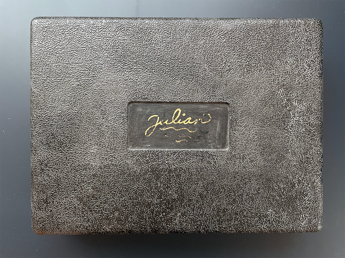
My adventure started probably around 8 years old, when one of my uncles gave me a gift for my bday: a black box with my name written on the top. The excitement was electrifying (no pun). I slowly opened it up and inside were resistors, capacitors, LEDs, piezo buzzers, DC motors, buttons, batteries and, of course, candy. I played with that thing every second. I took it with me everywhere I went. I'd connect the buttons to LEDs, batteries and make motors spin. I was hooked. I knew I wanted to be an engineer and hack on hardware/software.
Fast forward a couple decades, I ended up graduating with a degree in Electrical Engineering and I was ready to party.
How It All Started
I started working at Xilinx as a silicon verification engineer and then later on transitioned to software engineering. Xilinx makes these fancy chips called FPGAs, that can be programmed in the field, to run almost any digital circuit. Initially, part of my job description included creating and running a wide variety of test patterns on the FPGAs, to test every available feature and interconnect routing path. Our goal was always to try and hit 100% test coverage and ensure that the devices we shipped out worked to spec.
The primary tool our team used for running verification test patterns was a small form-factor, FPGA-based benchtop tester. It ran painfully slow at single MHz speeds. It had no user interface or test program management system. Probably worst of all was that the test vectors executed directly from the Linux kernel, which led to really bad signal jitter. However, even with all its shortcomings, it was an invaluable tool that helped us catch countless bugs without having to get expensive tester time on the Automatic Test Equipment (ATE) machines and wait for data acquisition. Most importantly, it was easy to use and didn't require extensive configuration.
We constantly generated new test patterns and ran them around the clock. If the benchtop tester didn't end up catching any issues, the false positives would just show up when running full test programs on the ATE, thus removing any risk. As you can imagine, our iterative debug cycle was lightning fast. It was game changing. However, I saw that there was room for improvement — features that could literally save the company millions of dollars. So I quit and decided to build a better benchtop tester...
The Hardware
At first, I was very skeptical that it was even possible to take on such a complex project alone. Around that time, Andrew "bunnie" Huang unveiled the Novena computing platform, which absolutely blew my mind. I'd been following Bunnie's work since the Xbox days — check out his book — and he was always a huge inspiration to me. I'm obviously nowhere near Bunnie's level, but seeing the hardware he produced gave me the confidence I needed to start.
To learn PCB design, I scrutinized the Novena's schematic and PCB layout. I also studied many other popular open-source hardware projects, like the MicroZed, to try and learn how the pros do it. I also watched many of Robert Feranec's Fedevel videos on YouTube and ended up taking his Advanced PCB Layout Course. Robert is a PCB layout master — I highly recommend his videos and courses. Doing this prep work was honestly quite challenging and took a long time, but it was worth it and it created a foundation for what was to come.
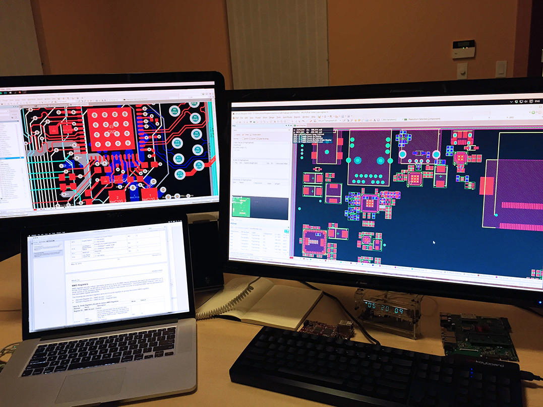
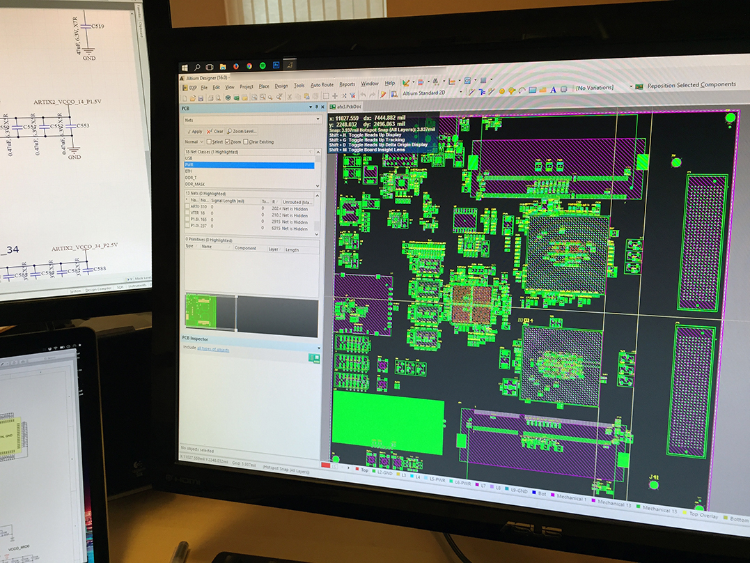
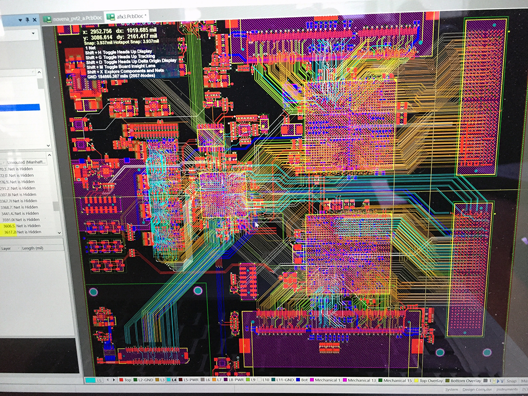
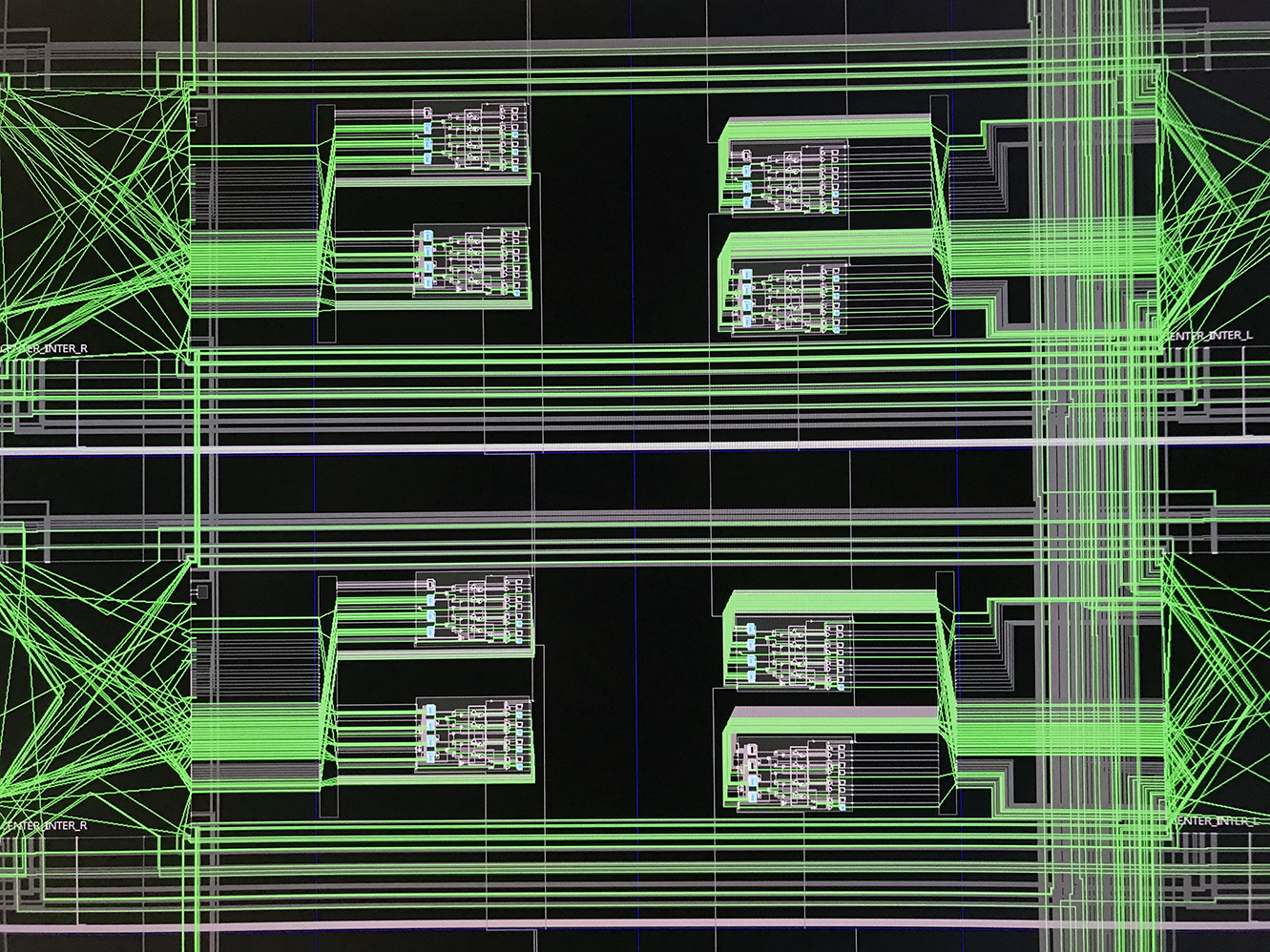
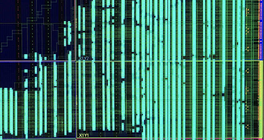
I started the board by going through a high-level planning phase to figure out what features, interfaces and bus architecture I wanted it to have. From there, I started the board architecture, selecting which chips to use and figuring out what my power budget was going to end up looking like. I read dozens of datasheets, created footprints, looked at reference designs and eventually I started the component placement phase. Eventually, I had to get stack-ups from the board houses, so I could calculate the trace dimensions to achieve the desired target impedance for certain nets. Even with 12 layers, the layout was very challenging. The FPGAs are fine-pitch BGAs with high pin counts. After countless hours, I finished routing the last net, passed DRC and I was done with the design.
Below is a non-exhaustive list of what I had to research in order to complete the hardware portion of the project.
Hardware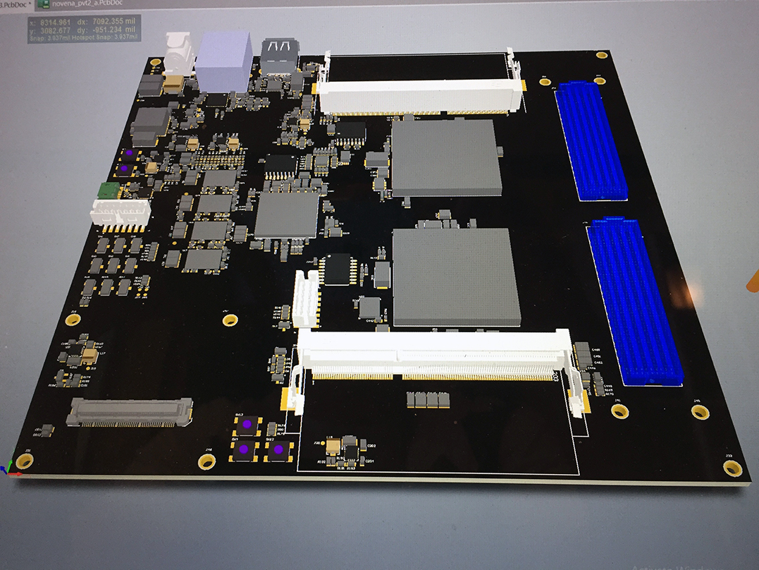
- board architecture
- power design and power sequencing
- schematic capture
- component selection and bill of materials (bom)
- 12-layer pcb placement and routing
- board stack-up and impedance calculation
- high-speed signal design
- strapping pins, pull-ups, pull-downs, open-collector, open-drain
- speccing bypass caps and resistors
- DDR3 fly-by-routing
- single ended and diff pair length matching
- datasheets, errata, routing, layout, etc... for Zynq SoC, Artix FPGA, Gigabit Ethernet, USB 2.0, JTAG, UART, I2C, SD Card, SPI
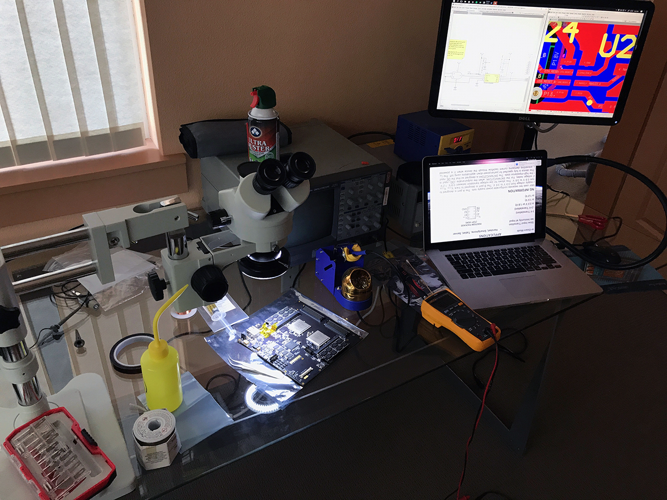
- debug and rework using DMM, oscilloscope, microscope and microsoldering iron
The Tools
In regards to software tooling, I was debating on whether I should use KiCad or Altium Designer. Ultimately, I ended up using Altium Designer for schematic capture and pcb layout, since that's what Bunnie and Robert both used and for such a complicated 12-layer board, I was afraid that KiCad didn't have the features I needed.
I also ended up acquiring all the physical tools below, as the project progressed and the need arose.
- Hakko FR810B-05 SMD Hot Air Rework Station
- Polyimide Film (Kapton) Tape
- Hakko Hot Air Nozzle, N51 Series, 2.5mm
- Aven 17542 Desoldering Wick, 2.5mm Width, 5' Length
- Kester 24-6337-0010 44 Rosin Core Solder 63/37 .020 1 lb. Spool
- AmScope SM-4TZ-144A Professional Trinocular Stereo Zoom Microscope
- Hakko FM2032-51 Micro Soldering Handpiece
- Hakko Solder Tip, Conical, R0.1 x 6mm, Micro, FM-2032
- Hakko FM203-01 Soldering Station, Digital, ESD Safe, 2Port
- Digilent JTAG-HS3 Programming Cable
- Magnetic Wire
- Electronic Wipes
- AMTECH NC-559-V2-TF no-clean tacky solder flux (ROL0) 10cc kit USA 16150K
- Rigol DS2072A Digital Oscilloscope
The Software
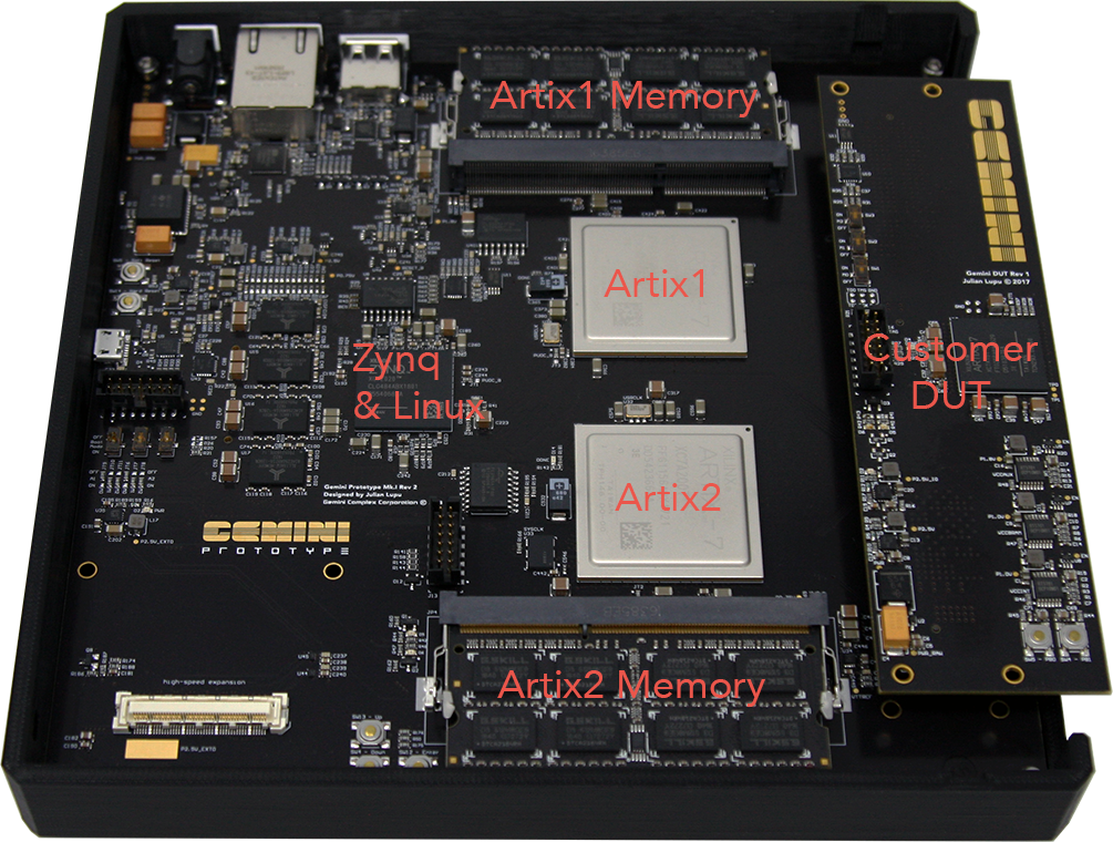
After finishing the board, I began working on the software and RTL code. For this part of the project, my goal was initially to implement a read/write/crc memory test for the artix units. So the idea was to get data from Linux, to a dma core, to IP running on the Zynq chip, to the IP running on the Artix and into Artix DDR3 memory. Once the memory was loaded up, the Artix IP would read the data, run crc, and write the calculated CRC back to memory. In Linux, a program would read the data back, and compare the CRC to a known value. This took a very long time to get running since it involved so many pieces coming together in perfect harmony. After getting this to work, I then focused on expanding the Artix IP core with a custom vector processing unit that would be responsible for executing test vectors from local Artix memory, and testing the connected customer DUT.
I've listed out below, as I did above, what I had to end up working on in regards to the firmware, to give you an idea of what's involved.
- build system using GNU make
- ARM GCC cross-compiler toolchain
- U-boot bootloader
- Linux kernel
- device-tree file (no bios)
- BusyBox
- root file system
- Linux kernel gcore driver written in C (Linux DMAEngine API, ioctl) to interact with the fpga GVPU IP core
- libgcore library written in C to interact with Linux gcore driver
- Leda the test pattern compiler
- on-board Python website for UI + sqlite db
- bring-up and getting all drivers to work with on-board interfaces
- Verilog/SystemVerilog
- Tcl for interacting with Vivado
- finite state machine design
- AMBA AXI4 and AXI4-Stream
- multi-clock cross domain crossing (CDC) design
- behavioral simulation
- simulation in c++ using Verilator
- static timing analysis
- Subcore IP block
- Agent IP block
- Memcore IP block
- Gemini Vector Processing Engine (GVPU) IP block
The Prototype
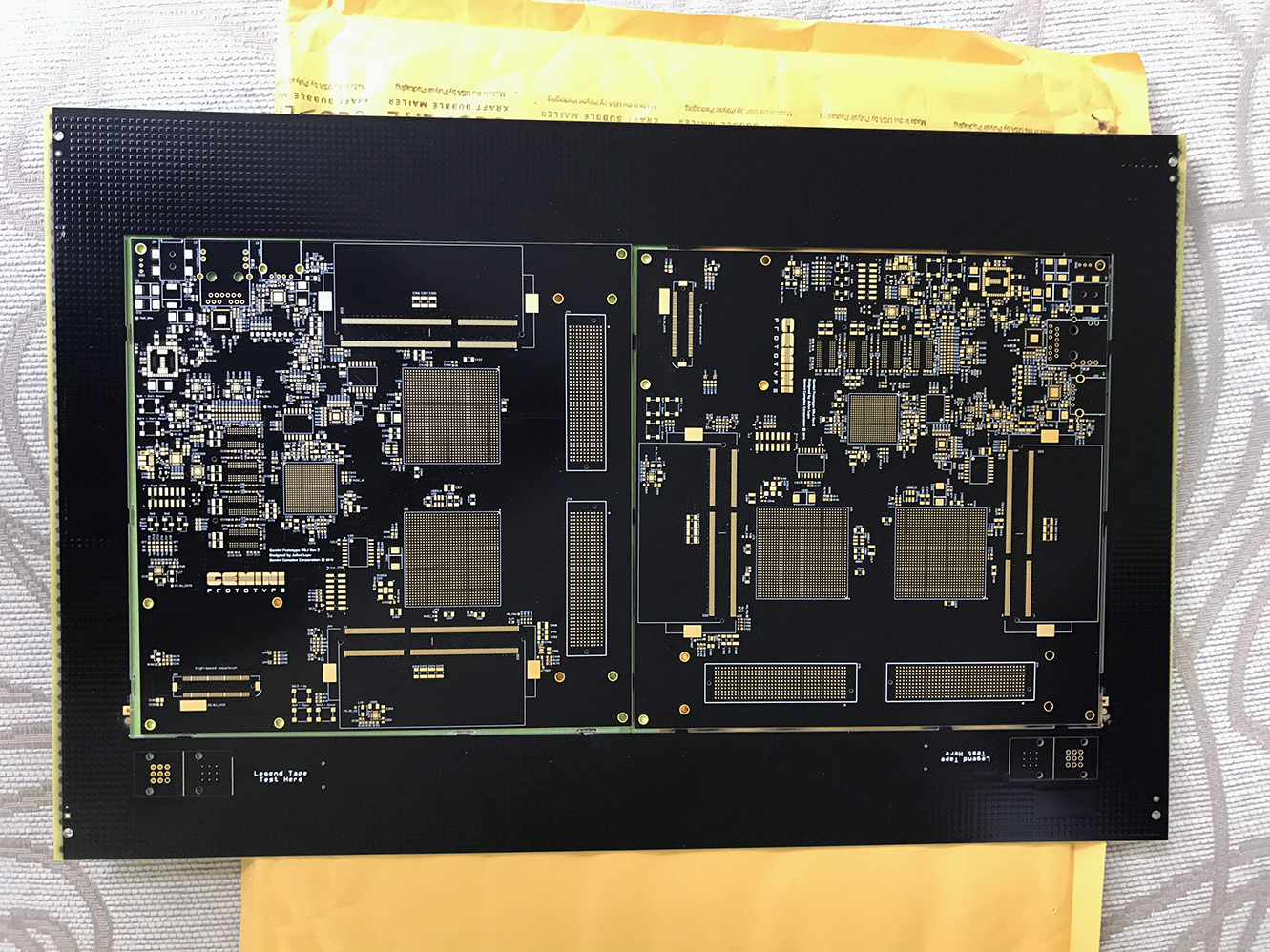
After finally finishing the layout, passing DRC and double/triple checking everything, it was time to get the board manufactured. I ended up using Sierra Circuits in Sunnyvale, CA, since I wanted to manufacture the board in the US. I have to say, their quality is on point. I was very pleased with the results.
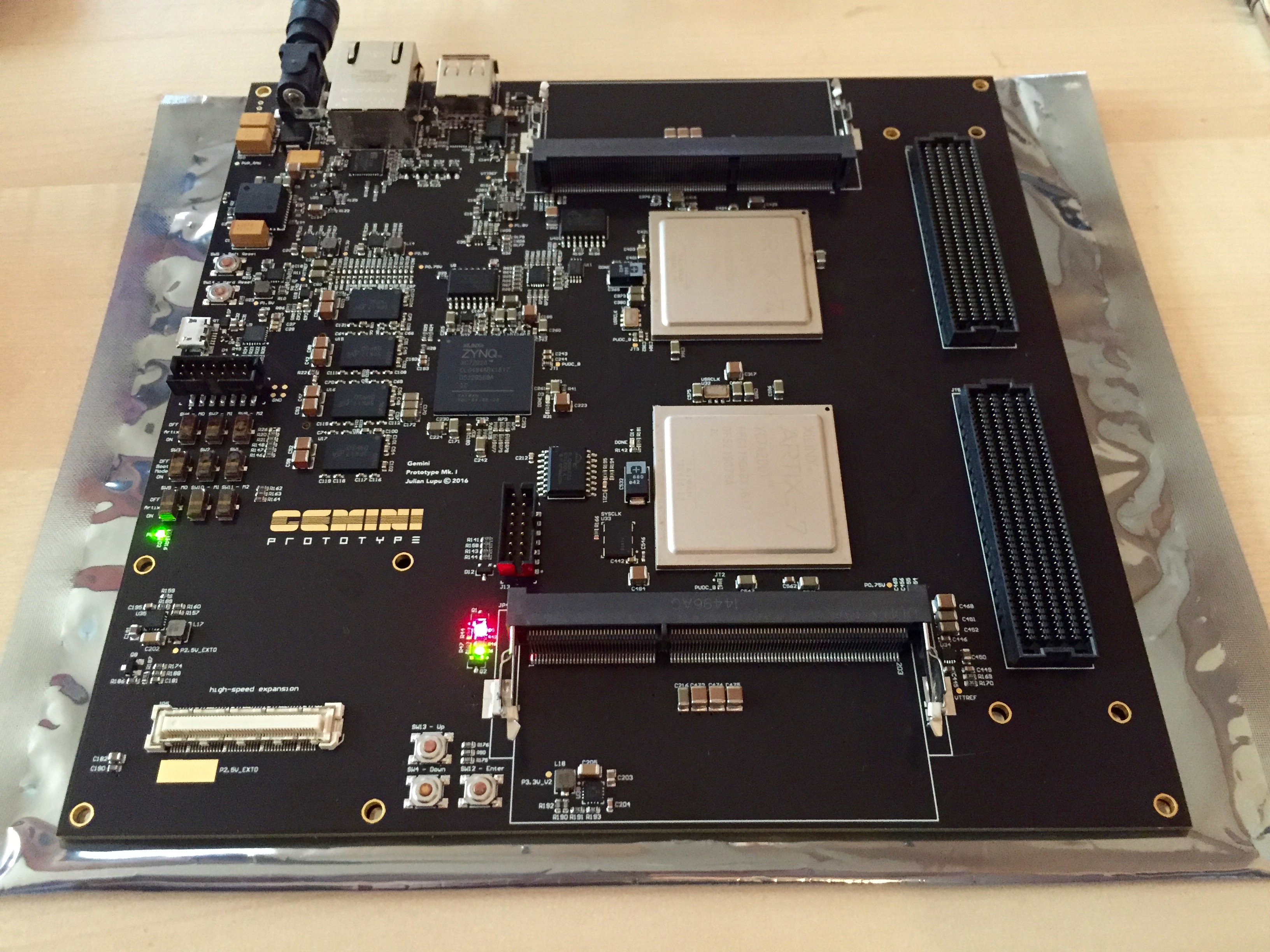
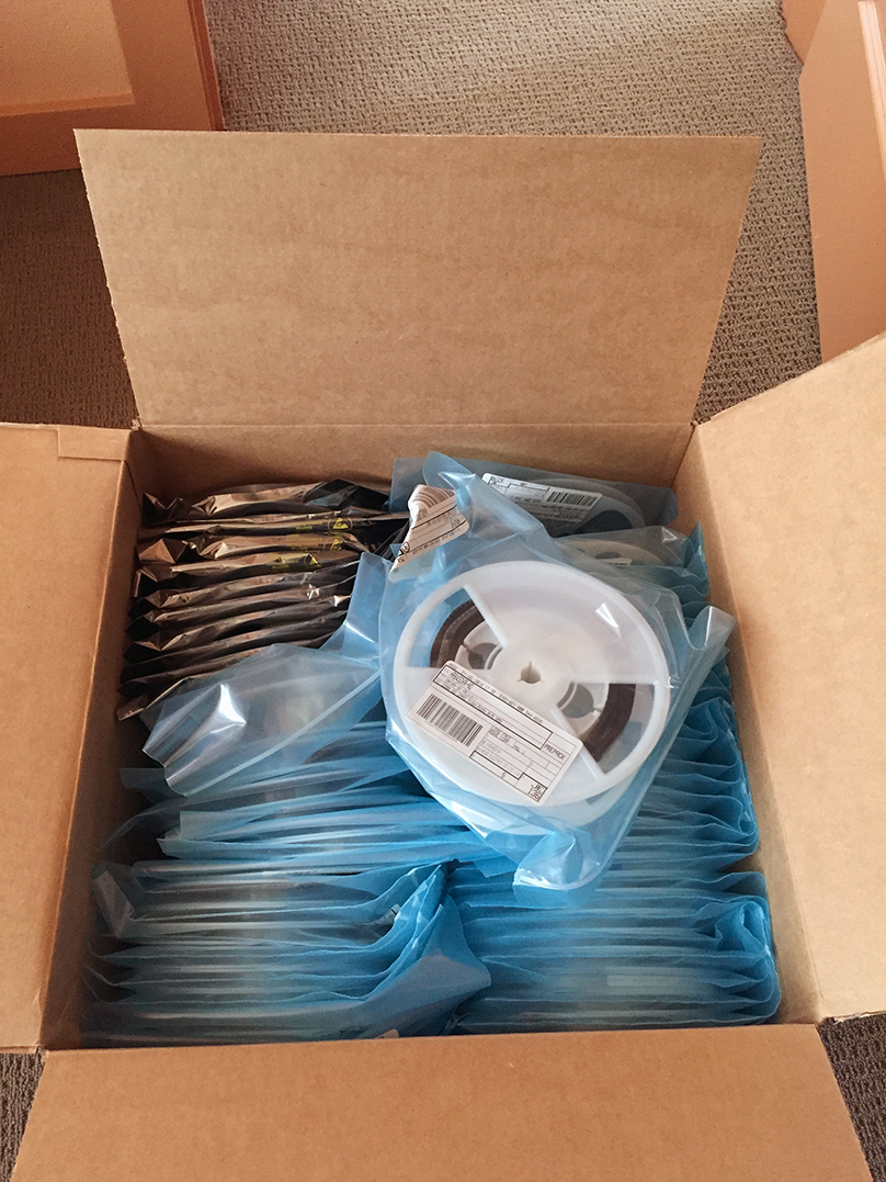
After getting the bare boards back, it was time to assemble them. I ordered all the parts from Digikey and Mouser, and shortly thereafter I got a giant box with reels of parts, which I shipped off to Sierra's assembly house. I then waited a few days and they shipped me back a giant box with the assembled boards. I was definitely anxious, not knowing if the boards would even power up, but power up they did.
I was quite happy with how the board turned out. I reached my first huge milestone and it it felt amazing. Next up was doing bring-up, rework, coding, and more.
The Storm
I could write a book about everything I had to end up debugging, but for brevity's sake, I'm just going to briefly touch on some of the major challenges that I came up against.
For me, the toughest part of this entire project was the FPGA firmware. Meeting setup and hold timing requirements given multiple fpgas, correctly forwarding clocks and signals externally off-chip, fixing clock domain crossing (CDC) issues and just generally debugging HDL bugs was straight up a nightmare. The ZipCPU creator rightly calls this FPGA Hell. Of course, this was also the area that I had the least amount of experience in. I was scouring Xilinx's Forums for answers almost daily. Almost every single time I found a helpful answer, it would be from a user named Avrum. This guy, in my opinion, is the Yoda of FPGA engineering. He knows his stuff and his posts helped me out greatly.
I was honestly so spoiled coming from software, where you can just quickly rerun a Python script or do a quick recompile. One does not simply "recompile" an RTL project. You have to do synthesis, place and route and simulation, which can take an absurd amount of time. After waiting for a very long time, your timing doesn't close and you have to go back and figure out why the critical timing path is having issues.
I had to end up learning all these tricks from the masters. I have a lot respect for actual chip designers that work on timing and design. It's a little easier on FPGAs, because it already has on-chip resources, like balanced clock trees, that are more-or-less guaranteed to work if following certain guidelines.
Here are two amazing tools that came in handy: Circuit Lab and EDA Playground. The former was primarily used to help me test out ideas while doing the board's schematic capture. And the latter gives you access to industry standard commercial simulators for free! The catch is that there is a limit on the file size, but it's still useful.
Here's a fantastic guide showing you how to do FPGA design with SystemVerilog. I highly recommend you check this out.
In regards to timing, your design is running on silicon where three major things can drastically impact the propagation of signals and consequently the peak performance: process, voltage and temperature. To meet timing, your final design must work at the worst and best case extremes of PVT variations. Imagine writing a Python script that only works at room temperature. I'm not going to go super deep on this, since it is most definitely out of the scope of this write-up. I'll just leave this here. All I'm going to say is heavily invest your time into properly doing simulation, mastering your synthesis tool's constraint system and static timing analysis tool sooner rather than later.
As the project progressed, I eventually got the simulation running the entire project's code, all the way from the userland C application and library, down to running the fpga verilog RTL in a chip pthread, thanks to Verilator. I was able to replace the Linux driver ioctl and dma calls with code that talked to the chip directly over AXI bus software calls.
There were many other challenges that I faced; especially getting vector data to correctly move from the kernel to the dedicated tester memories and getting the Gemini Vector Processing Unit to correctly execute vector instructions. I was able to slog through these challenges and I gained a tremendous amount of experience doing this.
The End
If you've gotten this far, you're absolutely crazy, but I commend you. Really, my goal with this post is to document and to show what went into making this product a reality. Did I bite off more than I can chew? Definitely. But, did I end up learning a lot? Most Definitely. However, I hope my post didn't dismay or bore you. On the contrary, I hope it sparked at least some small flicker of excitement. If you're interested in getting into electronics and FPGAs, I think one of the best ways to start is by getting your feet wet with a Lattice iCE40 board. Then write some simple Verilog to blink some LEDs using a finite state machine and get it to configure using the open-source FPGA toolchain called IceStorm. From there you can start working on progressively more challenging projects to level up your skills. From there, sky's the limit.
I hope you enjoyed the ride. Until next time...